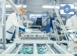
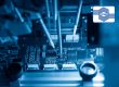
Through several long and expensive clean room processes, “wafers” are transformed into “smart” electronic microprocessors and chips. These chips can’t do anything by themselves and need to be integrated onto a printed circuit board (PCB) to be able to do something in the end (like operate your computer or telephone). This is what electronics PCB assembly is about.
The term printed circuit board assembly or PCBA refers to the process of mounting various electronic components onto a printed circuit board to develop and complete a fully functional printed circuit assembly. To help you get your head around the PCBA process, we have prepared this step-by-step overview of the standard electronics PCB assembly process.
TYPES OF MOUNTING TECHNOLOGIES
Step 1: Solder Paste Screening
The first step in the PCBA process is the application of solder paste to the bare PCBs through a solder paste printer. A stainless-steel stencil or solder screen is used to ensure that the solder paste is accurately deposited over the pads where surface-mount components will be placed.
Step 2: Machine Placement
Once the solder paste is applied, the prepared PCB is transported to an automated pick and place machine, which mounts the surface-mount components on the corresponding pads. The tension of the solder paste is sufficient to hold the components in place.
Step 3: Reflow Soldering
Once the components are all in place, the PCB is passed through an oven or a reflow soldering machine. This is done to solidify the solder paste, ensuring that the components are bound firmly to the board.
THROUGH-HOLE ASSEMBLY PROCESS
Step 1: Component Insertion
Depending on the board, it may depend upon through-hole components in addition to surface-mount components. The first step of through-hole assembly is to insert components into the corresponding positions accurately.
Step 2: Wave Soldering
In this step, the board is passed through a conveyer where it moves over a “wave” of molten solder so that the components can be professionally soldered to the circuit board.
Optical Inspection
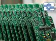
In both surface mount and through-hole constructions, each board is individually inspected to ensure quality.
Final Test
A thorough test is performed for the finished PCB for its functionality before it leaves the assembly line.
ATMWA is Australia’s premier electronics PCB solutions provider. We can handle designs and requirements of all types, and we encourage prospective clients to get in touch with us for any questions that might not be captured in this brief overview of, The Electronics PCB Assembly Process.