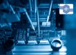
The technological universe is ceaselessly advancing. As our tools and devices become more sophisticated, the foundational elements powering them — particularly printed circuit board assemblies (PCB Assemblies) — are undergoing groundbreaking innovations. A cornerstone in maintaining the superior quality of PCB Assembly in today’s era is quality management, and this is where Automated Optical Inspection (AOI) stands out.
Understanding AOI in the Context of PCB Assembly
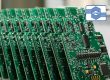
PCB Assembly, the process of mounting and connecting components onto a PCB, is a delicate and intricate operation. As we scale the peaks of technological advancement, the components get smaller, and the assemblies become denser. Every minute detail, every tiny solder joint, every connection becomes critical to the successful function of the end product. Enter Automated Optical Inspection (AOI).
In the realm of PCB Assembly, AOI stands as an invaluable guardian, ensuring every component is inspected by fully automated high-definition cameras for defects and inconsistencies.
The Essence of AOI
Automated Optical Inspection (AOI) is essentially a computerized visual inspection system. At its core, AOI uses a series of high-definition cameras that take precise images of the PCB Assembly from multiple angles. These images are then processed and compared with predefined or learned standards to detect any deviations or defects.
Beyond Just Cameras
While the cameras play a pivotal role, the real magic happens within the algorithms that process these images. Modern AOI systems utilize advanced machine learning and pattern recognition techniques. These algorithms not only identify blatant defects but also subtle nuances that could indicate potential future failures. Over time, as more PCB Assemblies are inspected, these systems can learn and adapt, increasing their detection accuracy.
The Evolution from 2D to 3D
The earlier AOI systems operated primarily on a 2D plane. They captured images of the PCB Assembly from a top-down perspective, ensuring components were present, correctly oriented, and properly soldered. While effective, these 2D systems had limitations, particularly when it came to detecting defects like lifted leads or solder joint quality beneath components.
However, as PCB Assembly processes grew more complex, the AOI technology evolved to meet the demands. The introduction of 3D AOI systems marked a significant leap in inspection capabilities. By utilizing multiple cameras and sometimes even lasers, 3D AOI systems can capture depth information, creating a topographical map of the PCB Assembly. This allows for a more comprehensive inspection, including the detection of co-planarity issues, volume, and distribution of solder paste, and even minute height variances across the assembly.
Ensuring Unparalleled Accuracy
The shift from 2D to 3D AOI, combined with advancements in image processing and machine learning algorithms, has granted modern AOI systems unparalleled accuracy. These systems can now identify defects as minute as a fraction of a millimeter, ensuring that PCB Assemblies are of the highest quality before they move to the next stage in production.
AOI’s Evolution in the PCB Assembly Line
Incorporating AOI into the PCB Assembly process introduces an era defined by precision and meticulousness. Modern AOI systems, equipped with high-resolution cameras and a fully telecentric lens, generate premium quality images of the PCB Assembly under review. When this imaging prowess is paired with sophisticated algorithmic technology, which perfectly blends 2D with shadow-proof 3D views, the AOI delivers an all-encompassing examination, leaving no stone unturned.
Present-day AOI systems are celebrated not just for their pinpoint accuracy but also for their remarkable speed. Consider our leading-edge AOI: it impressively inspects at a rate of 100cm2/second. Such efficiencies ensures that a wide range of possible defects, from missing components to intricate ones like lifted leads or head-in-pillow issues, are detected promptly. The addition of foreign material detection ensures that every element of the PCB Assembly is as it should be.
To ensure reliability, our AOI boasts the Escape Tracker, a self-checking mechanism. This feature minimizes human-induced errors by notifying operators of any programming discrepancies in real-time.
Addressing the varied demands of clients, our AOI showcases adaptability. It comes with an integrated IPC class setting, transitioning seamlessly between Classes 1, 2, or 3, catering to different PCB Assembly requirements.
In the spirit of transparency, our AOI offers a Barcode and Data Matrix reader, enabling complete traceability for each PCB Assembly. Once a defect is spotted, its specifics are stored securely offline. A quick barcode scan provides immediate insights, and a comprehensive report can be dispatched to clients as needed.
Why Opting for an AOI-Integrated PCB Assembly Partner is Crucial
In the current landscape of PCB Assembly, integrating AOI is not a luxury but an essential. The intricacies of modern PCB Assemblies demand an inspection method beyond manual checks. AOI, with its blend of speed and precision, stands head and shoulders above traditional methods.
Selecting a PCB Assembly partner like Advanced Technology & Manufacturing equipped with state-of-the-art AOI technology ensures the receipt of PCB Assemblies that epitomize quality. This not only minimizes potential challenges down the line but also enhances brand trust and market reputation.
In the dynamic world of PCB Assembly, AOI is a beacon of precision and quality assurance. As PCB Assemblies remain central to tech advancements, AOI is non-negotiable in the production process. Connect with a ATMWA today a PCB assembly company who recognises and integrates AOI signifies a commitment to quality, forward-thinking, and excellence.
Call +618-9444-3288 for or visit us here.